
Table of Contents
If you were to zoom into a microchip, you would discover a nanoscopic city. It is a landscape of computing skyscrapers, hundreds of layers tall, connected by hundreds of kilometers of wires. At the foundation of this city lie the transistors—billions of them acting as the binary switches of our digital world. For over 50 years, the industry followed Moore’s Law, doubling the number of transistors on a chip every two years. But around 2015, this progress threatened to grind to a halt.
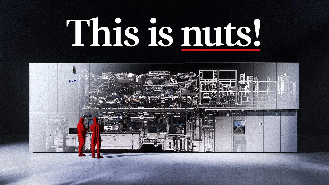
The physical limitations of light and materials suggested we had reached a hard wall. Yet, the industry broke through, thanks largely to a single company and a machine that many experts claimed was impossible to build. This is the story of ASML and the extreme ultraviolet (EUV) lithography machine—a device that costs over $350 million and represents perhaps the most complex commercial product humanity has ever engineered.
Key Takeaways
- EUV technology saved Moore’s Law: When traditional lithography hit physical limits, ASML successfully commercialized Extreme Ultraviolet light (13.5nm wavelength) to print smaller transistors.
- The engineering is staggering: The machine hits 50,000 tin droplets per second with a high-powered laser, vaporizing them into plasma brighter than the sun, with timing accuracy equivalent to hitting a golf ball into a hole 200 meters away.
- Mirrors replaced lenses: Because EUV light is absorbed by glass and air, the system operates in a vacuum using mirrors so smooth that if scaled to the size of Earth, the largest bump would be the thickness of a playing card.
- It required "unreasonable" persistence: The technology took over 30 years to develop, surviving funding cuts and widespread scientific skepticism to become the backbone of modern computing.
The Physics Wall: Why We Needed EUV
To understand why this machine exists, one must understand how chips are made. The process, known as photolithography, involves coating a silicon wafer with a light-sensitive material called photoresist. Engineers shine light through a patterned mask (reticle) to imprint a design onto the wafer, much like developing a photograph. The exposed areas are then etched away to create the physical structures of the chip.
The critical limitation here is diffraction. As chip features became smaller, the gaps in the mask approached the wavelength of the light being used. When light passes through such small openings, it spreads out, creating interference patterns rather than sharp lines. The industry standard was Deep UV light with a wavelength of 193 nanometers. By using tricks like water immersion and multi-patterning, engineers pushed this technology to its absolute limit.
To go smaller, the industry needed a shorter wavelength. The theoretical solution was Extreme Ultraviolet (EUV) light with a wavelength of around 13.5 nanometers. However, moving to EUV wasn't just an upgrade; it required reinventing the entire physics of lithography.
The Engineering Challenges of "Soft" X-Rays
EUV light, sometimes considered soft X-rays, behaves differently than the light used in previous generations. It is absorbed by almost everything—including air and standard glass lenses. This presented two massive hurdles that took decades to clear.
The Mirror Revolution
Because lenses absorb EUV, the machine cannot use refraction to focus light. Instead, it must use reflection. But EUV reflects poorly off standard surfaces. The solution, pioneered by researchers like Jim Underwood and Troy Barbee, involves multilayer mirrors based on Bragg reflection.
These mirrors are constructed with alternating layers of silicon and molybdenum. By tuning the thickness of these layers to exactly one-quarter of the light's wavelength, the small reflections from each boundary interfere constructively, creating a strong reflection. A typical mirror requires roughly 76 alternating layers to achieve about 70% reflectivity.
The precision required for these mirrors is difficult to comprehend. The surfaces must be atomically smooth to prevent scattering.
"If one mirror would be the size of Germany, the biggest bump would be about a millimeter high."
Furthermore, because each reflection loses about 30% of the light, and the system requires multiple mirrors to correct optical aberrations, only a tiny fraction of the generated light (often less than 4%) actually reaches the wafer. This necessitated a light source of immense power.
Building a Sun on Earth
The most difficult component of the EUV machine is the light source. Early attempts to generate EUV using electrical discharge plasma couldn't scale to the necessary wattage. ASML and their partners eventually settled on a method called Laser-Produced Plasma (LPP).
The process sounds more like science fiction than manufacturing:
- A generator shoots a microscopic droplet of molten tin into a vacuum chamber at speeds around 250 kilometers per hour.
- A high-powered CO2 laser blasts this droplet.
- The tin vaporizes into plasma reaching temperatures of 220,000 Kelvin—roughly 40 times hotter than the surface of the sun.
- As the electrons recombine with ions, they emit EUV light.
This violence happens 50,000 times every single second. The precision required is akin to shooting a golf ball through a tornado and landing it in a cup 200 meters away, every time, continuously.
The "Pancake" Breakthrough
For years, the power output was too low to be commercially viable. The breakthrough came when engineers decided to hit the tin droplet twice. Today, a pre-pulse laser hits the spherical droplet first, flattening it into a pancake shape. This increases the surface area. Microseconds later, the main laser pulse hits the pancake, vaporizing it more efficiently. This method drastically improved the conversion of laser power to EUV light, allowing the source to reach the necessary 200+ watts.
Managing the Debris
Exploding metal droplets 50,000 times a second creates a mess. If even a nanometer of tin debris were to coat the collector mirror, the $350 million machine would become useless. ASML solves this by blasting hydrogen gas through the chamber at hurricane speeds. The hydrogen reacts with the tin to form stannane gas, which can be pumped out, keeping the mirrors clean. Even the "cleaning" process required innovation; engineers discovered that injecting a precise amount of oxygen helped maintain the mirror's protective coating during operation.
The High-NA Era: Pushing Physics Further
While the first generation of EUV machines (Low-NA) is currently producing the world's most advanced chips, ASML has already developed the next generation: High-NA EUV.
Numerical Aperture (NA) determines the resolution of the optical system. The higher the NA, the smaller the features you can print. The new High-NA machines increase this metric from 0.33 to 0.55. This allows chipmakers to print smaller features with fewer manufacturing steps, reducing complexity and defects.
These machines are behemoths. A single High-NA system requires 250 shipping containers and three Boeing 747s to transport. Inside, the environment is controlled to a degree that makes a hospital operating room look filthy. In the cleanroom where these machines are assembled, there are fewer than 10 particles of 0.1-micron size per cubic meter.
Extreme Precision
The optical precision of the High-NA system is unrivaled. The Zeiss mirrors used in these machines are so accurate that if you were to shine a laser pointer from Earth to the Moon, the mirror control could determine whether you pointed at the left side or the right side of a dime placed on the lunar surface.
Conclusion: The Triumph of the Unreasonable
The development of EUV lithography was not a straight line. It was a 30-year odyssey filled with failure, skepticism, and financial peril. In the 1980s, when Hiroo Kinoshita first proposed using X-rays, he was laughed off the stage. When US researchers presented similar findings, they were told they would "never speak of it again."
EUV succeeded only because a small group of scientists and engineers refused to be reasonable. They persisted when the physics seemed impossible and the economics seemed foolish. They doubled down on investments when prototypes were failing. As the host of the source material noted:
"The reasonable man adapts himself to the world; the unreasonable one persists in trying to adapt the world to himself. Therefore, all progress depends on the unreasonable man."
Today, virtually every advanced piece of electronics—from the smartphone in your pocket to the servers running the internet—relies on chips made by the machine that "couldn't be built." It stands as a testament to the power of stubborn, collaborative engineering to push the boundaries of reality.


